Alarm|Sensor Cahaya
 |
| Rangkaian Alarm|Sensor Cahaya |
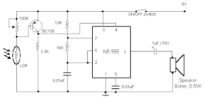
When no light falls on the LDR, the transistor is pulled high by the variable resistor. Hence the transistor is OFF and the reset pin of the 555 is pulled low. Due the this the 555 is reset. When light falls on the LDR, its resistance decreases and pulls the bases of the transistor low hence turning it ON. This pulls the reset pin 4 of the 555 high and hence enables the 555 oscillator and a sound is Produced by the speakers. The 100K variable resistor has to be adjusted to set the light intensity That triggers the alarm.
function of each pin:
- Ground, is the input pin of the negative DC voltage source
- Trigger, the lower the negative input comparator (comparator B) that maintain low voltage oscillation capacitor in third Fcc and set RS flip-flop
- Output, the output pin of the IC 555.
- Reset, the pin which serves to reset the latch inside the IC which will affect the work to reset IC. This pin is connected to a PNP-type transistor gate, so the transistor will be active if given a logic low. Normally this pin is connected directly to avoid reset Fcc
- Control Voltage, this pin serves to regulate the stability of the negative reference voltage input (comparator A). This pin can be left hanging, but to ensure the stability of the reference comparator A, usually associated with the order of about 10nF capacitor to pin groun
- Threshold, this pin is connected to the positive input (comparator A) which will reset the RS flip-flop when the voltage on the capacitor started to exceed 2 / 3 Vc
- Discharge, this pin is connected to an open collector transistor Q1 is connected to ground emitternya. Switching transistor serves to clamp the corresponding node to ground at a certain timing
- VCC, this pin to receive a DC voltage supply. Usually will work optimally if given a 5-15V. the current supply can be viewed in a datasheet, which is around 10-15mA.


0 comments:
Post a Comment