This is default featured post 1 title

Go to Blogger edit html and find these sentences.Now replace these sentences with your own descriptions.This theme is Bloggerized by Lasantha Bandara - Premiumbloggertemplates.com.

This is default featured post 2 title

Go to Blogger edit html and find these sentences.Now replace these sentences with your own descriptions.This theme is Bloggerized by Lasantha Bandara - Premiumbloggertemplates.com.

This is default featured post 3 title

Go to Blogger edit html and find these sentences.Now replace these sentences with your own descriptions.This theme is Bloggerized by Lasantha Bandara - Premiumbloggertemplates.com.

This is default featured post 4 title

Go to Blogger edit html and find these sentences.Now replace these sentences with your own descriptions.This theme is Bloggerized by Lasantha Bandara - Premiumbloggertemplates.com.

This is default featured post 5 title

Go to Blogger edit html and find these sentences.Now replace these sentences with your own descriptions.This theme is Bloggerized by Lasantha Bandara - Premiumbloggertemplates.com.

Saturday, March 31, 2012

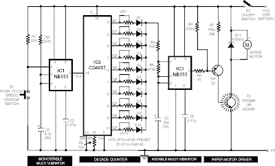
Rangkaian Kontrol Kecepatan Wiper Mobil

For some car wiper speed sometimes just made some speed so that less appropriate when we want a different speed, but for those of you who want a digital wiper speed controller you can also use this circuit to replace your old system.

rangkaian kontrol kecepatan wiper mobilSkema rangkaian kontrol kecepatan wiper mobil

This circuit comprises 2 timer NE555 ICs, one CD4017 decade counter, one TIP32 driver transistor, a 2N3055/ TIP3055 power transistor and A Few other discrete components. Timer IC1 is configured as a mono-stable multivibrator produces a pulse Pls Which one presses switch S1 momentarily. This pulse acts as a clock pulse for the decade counter (IC2) Which advances by one count on Each successive clock pulse or the push of switch S1. Ten presets (VR1 through VR10), for Different sets of values by trial and error, Are Used At The ten outputs of IC2. But since only one output of IC2 is high at a time, only one preset (selected at the output) effectively comes in series with resistors R4 and R5 timing connected in the circuit of timer IC3 Which functions in astable mode. As presets VR1 through VR10 are set for Different values, Different time periods (or frequencies) for astable multivibrator IC3 Can be selected. The output of IC3 is applied to the pnp driver transistor TIP32 for driving the final power transistor 2N3055 Which in turn drives the wiper motor at the selected sweep speed. The power supply for the wiper motor as well as the circuit is tapped from the vehicle s battery Itself. The duration of the monostable multivibrator IC1 is set for a period of nearly one second.

Source : www.electronic-circuits-diagrams.com

Solar Charger Circuit

Here is an Energy saving battery charger. It harvests solar energy to replenish 12 volt Inverter battery. It has auto cut off facility to stop charging when the battery attains full charge. The charger uses a 24 volt solar panel as input.

The circuit uses a variable voltage regulator IC LM 317 to set the output voltage steady around 16 volts. Variable resistor VR controls the output
voltage. When the solar panel generates current, D1 forward biases and Regulator IC gets input current. Its output voltage depends on the setting of VR and the output current is controlled by R1.This current passes through D2 and R3. When the output voltage is above (as set by VR) 16volts, Zener diode ZD2 conducts and gives stable 15 volts for charging. Charging current depends on R1 and R3. Around 250 to 300 milli ampere current will be available for charging. Green LED indicates charging status. When the battery attains full voltage around 13 volts, Zener diode ZD1 conducts and T1 forward biases. This drains the output current from the regulator IC through T1 and charging process stops. When the battery voltage reduces below 12 volts, ZD1 turns off and battery charging starts again.


Connect the circuit to the solar panel and measure the input voltage. Make sure that it is above 18 volts. Connect the circuit to the battery with correct polarity and adjust VR till LED lights. This indicates the conduction of ZD2 and output voltage. Use heat sinks for LM317 and TIP 122 to dissipate heat.
Note : The same circuit can be modified for charging different types of batteries. The only modification required is the change of ZD1 and ZD2. Select ZD2 value for the required output voltage and ZD1 for cut off voltage level. For example for 6 volt battery, ZD1 should be 6.1 volts and ZD2 6.8 volt. For Mobile battery, ZD1 should be 4.7 volts and ZD2 5.1 volts. All the other components remain same.

Touch volume control circuit

Touch controls are not only used to switch devices on or off. They can also be used to control different functions. One good example is the TV remote control. If it is very important to keep the activated functions for a long period of time, it is always better to use a digital memory system. However, if small drifts in the control status is acceptable, a simple analog design can be used to memorize the status.


The touch volume controller is one such analog memory touch control switch. The main function centers mostly on the IC1. It is an opamp configured as an integrator with a high impedance input. If sensor 1 is touched, the capacitor C2 charges through the skin resistance and voltage at the output of IC1 decreases linearly until it reaches zero volt. Touching the other sensor (sensor 2) will produce the opposite result: the voltage at the pin 6 of IC1 will increase linearly until it reaches the power supply level. The special function of this touch volume control circuit is that after moving your finger away from the sensor(s), the output voltage of IC1 stays at that level.
This voltage value is memorized by C2. This analog memory however has a problem in long time periods: The voltage value drifts away by 2 % per hour due to the unavoidable current leak in the capacitor. To improve this situation, it is highly recommended to put this circuit in a moisture proof box.
This touch volume controller circuit has a wide application range. It can be used in devices where a potentiometer can be controlled through voltage levels. The touch sensors can alse be replaced with conventional push button switches. The capactiors C1 and C4 are very important in the circuit: they prevent the IC1 from oscillating. Simultaneously closing both switches will not damage the circuit.

Touch volume control PCB layout


Rangkaian Saklar Tepuk (Clap Switch Circuit)

A clap switch circuit is a classic beginner’s project. Equipment can be switched on and off by just clapping your hands. Add a tiny microcontroller and you can easily build-in some more useful features.
The microcontroller in this circuit makes it a simple job to add some useful features that are not seen on other clap switch designs:


– Changeover relay contacts enable the unit to be wired in conjunction with a manual changeover switch so
that manual override of the switched equipment is always possible.
– The unit is only responsive to a specific sequence of sounds i.e., two claps within a defined time window.
– A safety feature masks the input for a given time window if misuse (repeated commands) is detected (useful if children have discovered how it works).
The safety feature and two-clap sequence detector can be built using TTL or CMOS flip-flops but by using a single microcontroller the circuit can be greatly simplified. A mains power supply is included so no additional power source is required.
The Microchip flash PIC12F629 microcontroller is a neat device; the small 8-pin package contains a complete microcontroller including clock generator, reset circuitry, Flash ROM, RAM and EEPROM. Two of the eight pins are used for the supply connections while the remaining six are general-purpose I/O pins. A few of these pins have special function like the comparator inputs. The sound sensitivity of the circuit can be adjusted by programming the comparator threshold level in software.

Clap switch COMPONENTS LIST:
Resistors:
R1,R6,R7 = 4kΩ7
R2 = 150kΩ
R3 = 22kΩ
R4 = 10kΩ
R5 = 150Ω
P1 = 100kΩ preset H
Capacitors:
C1 = 220μF 25V radial
C2 = 100nF
C3 = 1μF 16V
Semiconductors:
B1 = B80C1500 (round case, 80V piv, 1.5A)
D1,D2 = 1N4148
D3 = bicolour LED (red/green)
IC1 = 78L05
IC2 = PIC12F629CP, programmed
T1,T2,T3 = BC238 or BC547
Miscellaneous:
JP1 = 2-way pinheader with jumper
K1 = 2-way PCB terminal block, lead pitch 7.5mm
K2 = 3- way PCB terminal block, lead pitch 7.5mm
MIC1 = 2-terminal electret microphone capsule
Re1 = bistable relay, 2 x changeover (e.g., Schrack RT314F12)
Tr1 = mains transformer 1 x 6V, min. 2VA, short-circuit proof (e.g., Marschner VN30.15/10522 or Era 030-7340.0T; Conrad Electronics # 506141)

Thursday, March 29, 2012

NiCad Battery Charger Circuit

This array charger ambit is advised for recharging NiCad batteries based on an AC-powered accepted antecedent method. It can crank out as abundant as 1 amp and can be adapted to go alike college by allotment altered accessories for Q1. Since this ambit uses AC band voltages and currents, amuse exercise acute attention during assembly, turn-on,
and test. NiCAD batteries accept a accommodation blueprint alleged milliamp-hours. This amount alleged “C” is a admeasurement of how abundant absolute accepted they can accommodate in one hour. Milliamp-hours is addition way to accurate the activity independent in the battery. To recharge a NiCAD array conservatively, it is accepted convenance to pump a accepted of 0.1 C into the anode or absolute terminal for about 12 hours. Therefore, if you had a D-size NiCAD with a accommodation of 4000mAh, you would appetite to allegation it at 400mA for about 12 hours. Addition advantage of this charging address is that it is affable on batteries and doesn’t account them to lose accommodation as bound as the fast allegation techniques.
The achievement accepted of this array charger ambit is controlled by the accretion of the bandgap advertence diode and the base-emitter alliance of the PNP transistor. The PNP transistor provides abrogating acknowledgment to the aboideau of the MOSFET. As acclaimed in the schematic, the batteries actuality answerable can accept a absolute of 12V which is agnate to about 8 NiCAD’s in series. The achievement accepted is bent by the amount of R1 which is bent by:
R1=3.2Volts/Iout
The ability amusement of R1 will equal:
Pr1=3.2Volts*Iout
Be abiding to accommodate pleanty of heatsink for Q1 and accept an appropriately sized resistor for R1. The afterward table summarizes some of the resistor accepted combinations that are possible:
Iout Resistor Amount Resistor Power
100mA 33 ohms 1 watt
500mA 6.2 ohms 2 watt
1Amp 3.3 ohms 5 watt

Regulator 5A model Matahari

Skema Rangkaian Regulator 5Ampere ini mempunyai tegangan pengeluaran yang bervariasi dari mulai 3 Volt sampai 13.8 Volt yang di atur tegangannya oleh saklar rotari. Regulator ini sangat cocok untuk berbagai rangkaian, karena pengeluarannya sangat stabil dan tegangannya murni.

Wednesday, March 28, 2012

Kisah Tawakal Kepada Allah

Kisah Tawakkal Kepada Allah.Melanjutkan postingan di Taman Berbagi yang lalu yaitu Tawakal Kepada Allah maka pada postingan kali ini adalah sebuah ibrah yang semoga kita bisa mengambil pelajarannya yaitu sebuah kisah tawakal kepada Allah dan semoga kisah tawakal ini bermanfaat sahabat.

Ada sebuah kisah yang menarik dari seorang yang bernama Hatim Al-Asham.Suatu kali Hatim ingin menunaikan ibadah haji ke Baitullah.Ia pun mengumpulkan anak-anaknya dan berkata : "Saya akan pergi untuk menunaikan ibadah haji ke Baitullah." Anak-anaknya berkata : "Siapa yang akan memenuhi kebutuhan kami ?"Akan tetapi, salah seorang puterinya berkata dengan penuh keyakinan : "Wahai ayah, silahkan ayah pergi dan sempurnakanlah ibadah haji ayah.Karena saya yakin, ayah bukan pemberi rezeki."

Hatim pun pergi,selang beberapa hari makanan di rumah habis.Lalu seluruh keluarga datang kepada gadis bertakwa itu, dengan melontarkan cacian dan celaan.Kemudian gadis itu menyepi dan menautkan permohonannya kepada Rabbnya yang telah berfirman :
" Barangsiapa yang bertakwa kepada Allah,Dia akan menjadikan jalan keluar baginya dan memberinya rezeki dari arah yang tiada disangka-sangka...
( QS, Ath-Thalaq (65) : 2 - 3 ).

kisah tawakal,ibrah tawakal,taman berbagi

Demi Allah yang tidak ada Tuhan selain Dia, Dia tidak akan mengabaikan seorang yang bertakwa.Wujudkanlah takwa dan serahkan segala urusan kepada Raja.

Allah memenuhi permohonan si gadis.Pada saat yang bersamaan, pemimpin negeri itu sedang meninjau kondisi rakyatnya, ketika sampai di depan rumah Hatim, ia begitu didera rasa haus, yang hampir-hampir membunuhnya.Ia berkata kepada salah satu pengawalnya : "Carikan aku segelas air dingin." Maka pengawal itu masuk ke rumah terdekat, yaitu rumah Hatim.Para penghuni rumah pun segera menyediakan gelas yang bersih dan air yang dingin.

Sang Raja meminum air yang disediakan, ia bertanya : "Rumah siapa ini ?"Mereka menjawab : "Milik Hatim Al-Asham." Raja bertanya lagi : "Ia seorang yang shaleh ?" Mereka menjawab : "Benar". Raja berkata : "Segala puji hanya milik Allah yang telah memberi kami minum dari rumah orang shaleh.Dimana dia sekarang, agar kita memberi salam kepadanya ?" Mereka menjawab : "Dia pergi untuk menunaikan ibadah haji ke Baitullah." Raja berkata :" Kalau demikian, demi Allah, kita wajib mencukupi kebutuhan anggota keluarganya ketika dia tidak ada."

Kemudian sang raja mengeluarkan sekantong uang emas dan melemparkannya ke rumah Hatim Al Asham.Akan tetapi Allah yang Maha Memberi Rezeki hendak memberikan tambahan rezeki yang lain, Dia gerakkan hati sang raja.Raja menoleh ke arah para prajuritnya dan berkata : " Barangsiapa yang mencintaiku, hendaklah ia melakukan seperti tindakanku tadi ".Maka, masing-masing prajurit melemparkan semua harta yang mereka bawa, sebagai bentuk basa-basi kepada sang raja.

Akhirnya rumah si gadis penuh dengan emas.Si gadis masuk ke kamarnya sambil menangis haru, saudara-saudaranya keluar mendengar tangisannya." Kita telah menjadi manusia yang paling kaya.Seorang makhluk telah memandang ke arah kita sekali pandang, sehingga kita pun menjadi kaya, lantas bagaimana jika Sang Khalik yang memandang ke arah kita.

Saudara-saudaraku, inilah hakikat tawakal.Inilah keutamaan tawakal.Kita memohon kepada Allah agar menjadikan kita termasuk orang-orang yang bertawakal dan benar.Kita juga memohon kepada Allah agar mengaruniakan kepada kita manisnya tawakal kepadaNya dan kesejukan yakin kepada Allah serta nikmatnya kepercayaan kepadaNya.Sesungguhnya Dia-lah yang berhak untuk itu.Amin..Amin..Yaa Rabb.

Dan akhirnya semoga kisah tawakal kepada Allah ini dapat bermanfaat dan kita semuanya bisa mengambil pelajarannya aamiin.

Sumber : Menebar Kebaikan

Alarm Circuit For Motorcycle using CD4001


 Simple Alarm for motorcycle with a CD4001

This is a simple alarm circuit for a check with a 4001. You can use it to protect our home, motorcycle, car or any other application that comes to mind. In this circuit you will make a computer simulation with Livewire and then design the printed circuit Kicad.

OPERATION
SW1 is a normally closed switch when pressed triggers the flip-flop formed by the two NOR gates of the CD4001 and remains in that state for a time determined by the time constant of R5-C2. This time is the one who keeps the relay RL1 and operated by its two contacts that we investors will control two loads, for example a siren and a light or any other that we connect to P3 and P4.
After that time elapsed, the relay disconnects the circuit will soon be the alarm to be triggered again.
We can replace the switch Sw1 a PIR motion sensor, an infrared barrier, a smoke detector, gas detector, a magnetic sensor, a panic button or other device to act as a switch closed and opened fire at the alarm.
PRINTED CIRCUIT DESIGN
For the circuit we can only practical substitute for a preset R5 (RV1) so you can easily adjust the monitor while the charges.

Konverter 6 Volt ke 12 Volt


6V to 12VDC Converter Schematic
This inverter circuit can provide up to 800mA of 12V power from a 6V supply. For example, you could run 12V car accessories in a 6V (British?) car. The circuit is simple, about 75% efficient and quite useful. By changing just a few components, you can also modify it for different voltages.

Parts

PartTotal Qty.DescriptionSubstitutions
R1, R422.2K 1/4W Resistor
R2, R324.7K 1/4W Resistor
R511K 1/4W Resistor
R611.5K 1/4W Resistor
R7133K 1/4W Resistor
R8110K 1/4W Resistor
C1,C220.1uF Ceramic Disc Capacitor
C31470uF 25V Electrolytic Capcitor
D111N914 Diode
D211N4004 Diode
D3112V 400mW Zener Diode
Q1, Q2, Q43BC547 NPN Transistor
Q31BD679 NPN Transistor
L11See Notes
MISC1Heatsink For Q3, Binding Posts (For Input/Output), Wire, Board
Notes
1. L1 is a custom inductor wound with about 80 turns of 0.5mm magnet wire around a toroidal core with a 40mm outside diameter.
2. Different values of D3 can be used to get different output voltages from about 0.6V to around 30V. Note that at higher voltages the circuit might not perform as well and may not produce as much current. You may also need to use a larger C3 for higher voltages and/or higher currents.
3. You can use a larger value for C3 to provide better filtering.
4. The circuit will require about 2A from the 6V supply to provide the full 800mA at 12V.

Power Supplay 12 Volt Non Trafo


 This circuit will supply up to about 20ma at 12 volts. It uses capacitive reactance instead of resistance; and it doesn’t generate very much heat.The circuit draws about 30ma AC. Always use a fuse and/or a fusible resistor to be on the safe side. The values given are only a guide. There should be more than enough power available for timers, light operated switches, temperature controllers etc,
provided that you use an optical isolator as your circuit’s output device. (E.g. MOC 3010/3020) If a relay is unavoidable, use one with a mains voltage coil and switch the coil using the optical isolator.C1 should be of the ’suppressor type’; made to be connected directly across the incoming Mains Supply. They are generally covered with the logos of several different Safety Standards Authorities. If you need more current, use a larger value capacitor; or put two in parallel; but be careful of what you are doing to the Watts. The low voltage ‘AC’ is supplied by ZD1 and ZD2. The bridge rectifier can be any of the small ‘Round’, ‘In-line’, or ‘DIL’ types; or you could use four separate diodes. If you want to, you can replace R2 and ZD3 with a 78 Series regulator. The full sized ones will work; but if space is tight, there are some small 100ma versions available in TO 92 type cases. They look like a BC 547. It is also worth noting that many small circuits will work with an unregulated supply. You can, of course, alter any or all of the Zenner diodes in order to produce a different output voltage. As for the mains voltage, the suggestion regarding the 110v version is just that, a suggestion. I haven’t built it, so be prepared to experiment a little.

Rangkaian Detektor Signal AF/RF

The following circuit of special functions to detect the presence or absence of signal AF / RF. This circuit is very simple so as to make it requires a relatively low cost. Detektor Signal AF/RF circuit based an audio amplifier and a loudspeaker with a switch input to the AF and RF signal. The whole device can be made as small as possible so that it can be included in a container to keep the peace.

Audio amplifier section in this series created by IC TDA 2822M, with a low-power stereo amplifier in 8-pin mini-DIP. This IC is used as a bridge cofiguration to minimize output power up to 250 mW, the loudspeaker is in use 4 ohm, 500mW. Current required is less than 10mA with a 3V battery voltage.

Rangkaian Detektor Signal  AF/RF
Skema Rangkaian Detektor Signal AF/RF

List Component

R1 : 22K
R2, 3, 4 : 4K7
C1 : 1n
C2, 6, 7 : 0,1uF
C3, 4 : 10uF/16V
C5 : 0,01uf
D1 : OA79
VR1 : 22K
IC 1 : TDA2822M
LS : 8 ohm 500mW


When the switch in the AF position, Signal input audio input working on AF amplifier (IC 1 pin 7) via a capacitor C2 and Potentiometer VR1. Capacitor C2 is always holding the input amplifier of the DC voltage and make it happen in the audio signal frequency. Input signal IC 1 can be arranged with the help of potentiometer VR1.

When switch on the RF position, the detector and demodulator circuit formed by capacitor C1, diode D1, and resistors R1 and R2 are connected to the input rangakaian. When the audio signal is detected it will be significantly strengthened in kerangkaian for. Signal detection is done by plugging in tactile (probe) on the legs of the existing components.

Pengukur Suara Speaker

This circuit can be used to setup their home-cinema set adjusting all the loudspeaker outputs to the same level when heard from the listening position. The circuit is very simple (though linear and precise) ac millivoltmeter, using an existing multimeter set to 50 or 100µA fsd with the probes connected to J1 and J2 to read the results.

Rangkaian Pengukur Suara Speaker Skema Rangkaian Pengukur Suara Speaker


List coponent

R1................................... 10K 1/4W Resistor
R2,R3............................... 22K 1/4W Resistors
R4................................... 100K 1/4W Resistor
R5................................... 100R 1/4W Resistor
C1................................... 1µF 63V Polyester or Electrolytic Capacitor
C2................................... 100µF 25V Electrolytic Capacitor
C3................................... 220µF 25V Electrolytic Capacitor
D1-D4............................... BAT46 100V 150mA Schottky-barrier Diodes
IC1................................... CA3140 Op-Amp IC
MIC................................... Miniature electret microphone (See Notes)
J1,J2................................. 4mm Output sockets
SW1.................................. SPST Toggle or Slider Switch
B1................................... 9V

The precision of the measure is entirely depending on the frequency response of the microphone used but, fortunately, for the main purpose of this circuit an absolutely flat response is not required. Therefore, a cheap miniature electret microphone can be used.

Note:
Please be careful and set the volume control very low, to avoid loudspeakers' damage. Switch-on the Sound Pressure Level Meter and increase the volume of the amplifier in order to obtain an approximate center-scale reading. Repeat the same steps with all channels.

Rangkaian Loudness Aktif

Rangkaian Loudness Aktif
Skema Rangkaian Loudness Aktif
To get good audio reproduction at different listening levels, a different tone-setting controls should be necessary to suit the well known behavior of the human ear. In fact, the human ear sensitivity varies in a non-linear manner through the entire audible frequency band, as shown by Fletcher-Munson curves.

A simple approach to this problem can be done inserting a circuit in the Preamplifier stage, capable of automatically varying the frequency response of the entire audio chain in respect to the position of the control knob,
in order to keep ideal listening conditions under different listening levels .

Fortunately, the human ear is not too critical, so a rather simple circuit can provide a Satisfactory performance through a 40db range.


List Component Of Loudness Aktif

P1______________10K Linear Potentiometer (Dual-gang for stereo)

R1,R6,R8_________100K 1/4W Resistors
R2______________27K 1/4W Resistor
R3,R5____________1K 1/4W Resistors
R4______________1M 1/4W Resistor
R7______________20K 1/2W Trimmer Cermet

C1______________100nF 63V Polyester Capacitor
C2______________47nF 63V Polyester Capacitor
C3______________470nF 63V Polyester Capacitor
C4______________15nF 63V Polyester Capacitor
C5,C9____________1µF 63V Electrolytic or Polyester Capacitors
C6,C8____________47µF 63V Electrolytic Capacitors
C7______________100pF 63V Ceramic Capacitor

IC1_______________TL072 Dual BIFET Op-Amp

SW1________________DPDT Switch (four poles for stereo)


The circuit is shown with SW1 in the "Control-flat" position, ie without the Automatic Loudness Control. In this position the circuit acts as a linear Preamplifier stage, with the voltage gain is set by means of Trimmer R7. Switching SW1 in the opposite position the circuit becomes an Automatic Loudness Control and its frequency response varies in respect to the position of the control knob by the amount shown in the table below. C1 boosts the low frequencies and C4 boosts the higher ones. Maximum boost at low frequencies is limited by R2; R5 do the same at high frequencies.

Rangkaian Integrator Op-Amp 741

Op-amp is versatile electronic circuits are designed and specially packaged, so that by adding external components at all, can already be used for various purposes. One of them is to make the integrator integrator circuit functions to produce an output voltage which is an integral function of time from the input voltage.

Rangkaianintegrator widely used in the "analog computer" as a tool for solve the integral equation. This circuit can be made by placing capacitors at the input and output reversed and no-reverse input earthed. Input signal given to the input reversed.

Integrator Op-Amp 741Skema Rangkaian Integrator Op-Amp 741

Integrator circuit testing procedures
  • Arrange an op-amp integrators as shown in the image above. Supply Power dibua IC 741 can use two batteries or variable DC source.
  • Set the input signal from the FG to generate signal box 1 Vp-p on frequency of 1 kHz.
  • Use the oscilloscope to view the integrator output response
  • Based on the circuit as shown above, you will verify that the output and input will follow the equation

Rangkaian Penala Antena

This is a series of antenna-tuning circuit or circuits for transmitting antenna placement SW 3-30 MHz wave / short wave 3-30 Mhz. If the placement is just right then the maximum energy from the transmitter will send out all the antenna through sehinnga nothing is wasted. To get a clear picture of the circuit is click on the picture below.


Rangkaian Penala AntenaSkema Rangkaian Penala Antena


This transmacth circuit function is to locate an appropriate impedance between the transmitting antenna that occurred in the ratio 1:1 SWR reading it, because in this placement is associated with a series of SWR / standing wave ratio. Thus the purpose of 1:1 is the one that came out was also one emitted by the antenna instead of just half saja.Impedansinya generally is 50 Ohm. With this circuit the maximum power that can pass this circuit is 50 Watt.


About SWR meter

The SWR meter or VSWR (voltage standing wave ratio) meter measures the standing wave ratio in a transmission line. This is an item of radio equipment used to check the quality of the match between the antenna and the transmission line.

SWR Meter Installation SWR Meter Installation

SWR Meter
SWR Meter Pic


The VSWR meter should be connected in the line as close as possible to the antenna. This is because all practical transmission lines have a certain amount of loss, causing the reflected power to be attenuated as it travels back along the cable, and producing an artificially low VSWR reading on the meter.

Pengatur Kecepatan Motor Menggunakan PWM

So-called PWM or Pulse Modulation Witdh is a technique often used to control a load, for example, is the DC motor speed control, PWM techniques are often used.

Usually to make a simple PWM (for practice or introduction PWM) of the hobbyist to use some of the circuit made of Op-Amp, which consists of Schmitt Trigger circuit, integrator and comparator.

Diagram Pwm ControllerDiagram of PWM Controller


Schmitt Trigger function that produces a square wave will be converted by the integrator sawtooth wave or commonly also called Ramp, and Ramp compared with a reference voltage that can be changed much voltage. So the result is a PWM output.

Rangkaian PWM Motor/Light Controller
Skema Rangkaian Low Side PWM Motor/Light Controller

Rangkaian PWM Motor/Light Controller
Skema Rangkaian High Side PWM Motor/Light Controller


These two schematics are variations on another PWM circuit. The diagrams are for 12V operation only and there are high side (common ground) and low side (common +12V) versions. The low side version of the circuit uses an N Channel FET, the high side version of the circuit uses a P Channel FET. N Channel devices tend to handle more current than P Channel devices, they are also less expensive. The high side version of the circuit is useful when one side of the load has to be grounded.

This circuit can switch a fairly high amount of current, an IRFZ34N MOSFET can handle over 35 Amps if connected to a proper heat sink. Higher power FETs, such as the IRFZ48N or IRF1010Z can be substituted if even larger currents are required. It is also possible to connect multiple FETs in parallel for even more current capacity. Always use thermally conductive grease between the FET and the heat sink, and remember that the heat sink is electrically live.

Inductive loads (motors) may require special care since they can generate large voltage spikes that can damage the MOSFET. Replacing the 1N4002 with a fast recovery diode may help absorb the reverse voltage kick when driving an inductive load such as a motor. If you use these circuits for experiments with electric vehicles, be sure to install a circuit breaker in series with the battery, the circuit breaker should be easy to reach by the driver. This is especially important due to the fact that when MOSFETs fail, they often short out, leaving the motor on at full speed.

Multivibrator Astable Menggunakan IC 555

Multivibrator is an electronic circuit that at a certain time only one of two output voltage levels, except during the transition period. The transition (switching) between the two levels of output voltage occurs quickly. Two state level of the multivibrator output voltage, which is stable and Quasistable.
Astable multivibrator is called when the output voltage levels generated by the multivibrator circuit is quasistable. The circuit will only change the state of the output voltage level between the 2 conditions, each state has a fixed period. Multivibrator circuit will work independently and no longer need a trigger. Period of time each output voltage level is determined by the components making up the circuit.

The picture above is the astable multivibrator circuit. This circuit will work when the voltage applied to Vcc ration and ground her. This circuit has two conditions are always changing with time. Because changing the type is known as astable multivibrator. With constant changes of 0 and 1, then the multivibrator is also called a bistable multivibrator (multivibrator which has two stable state of 0 and 1).


This change in cycle length can be calculated using the following equation:

Period = t1 + t2
t1 = 0.7 x (RA + RB) XC
t2 = 0.7 xRBxC.

Rangkaian Multivibrator Monostable IC 555

Multivibrator Monostable IC 555
Rangkaian Multivibrator Monostable IC 555 is a pulse generator circuit in which the duration of the pulse is determined by the R-C connected to IC 555 timer. In such a vibrator, one state of output is stable while the other is quasi-stable (unstable). For auto-triggering of output from quasi-stable state to stable state energy is stored by an externally connected capaci tor C to a reference
level. The time taken in storage determines the pulse width. The transition of output from stable state to quasi-stable state is accom­plished by external triggering.

Capacitor C has to charge through resistance RA. The larger the time constant RAC, the longer it takes for the capacitor voltage to reach +2/3VCC. In other words, the RC time constant controls the width of the output pulse. The time during which the timer output remains high is given as

tp = 1.0986 RAC
where RA is in ohms and C is in farads. The above relation is derived as below. Voltage across the capacitor at any instant during charging period is given as


vc = VCC (1- e-t/RAC)
Substituting vc = 2/3 VCC in above equation we get the time taken by the capacitor to charge from 0 to +2/3VCC.

So +2/3VCC. = VCC. (1 – e-t/RAC) or t – RAC loge 3 = 1.0986 RAC
So pulse width, tP = 1.0986 RAC s 1.1 RAC
The pulse width of the circuit may range from micro-seconds to many seconds. This circuit is widely used in industry for many different timing applications.

Rangkaian Mixer Mini

 Although the modular Portable Mixer design available on these web pages has become a hit for many amateurs, some correspondents required a much simpler device, mainly for mixing mono signals.
This design should fulfil their needs, featuring three inputs with switchable high/low sensitivity and unusual level-control circuits, providing high overload margins and low-noise figures, proportional to gain-level settings.
Low current consumption due to a simple, five-transistor circuitry, allows the Mini Mixer to be powered by a common 9V PP3 battery for many hours.

Mini Mixer Parts:
P1,P2,P3_________5K Linear Potentiometers
R1,R11,R15_____180K 1/4W Resistors
R2,R12,R16_______2M2 1/4W Resistors
R3,R13,R17_____750R 1/4W Resistors (See Notes)
R4,R14,R18_______1K 1/4W Resistors
R5______________15K 1/4W Resistor
R6_____________220R 1/4W Resistor
R7_______________1K5 1/4W Resistor
R8_____________820R 1/4W Resistor
R9_____________150R 1/4W Resistor
R10____________100K 1/4W Resistor
C1,C6,C8_________1µF 63V Polyester or Electrolytic Capacitors
C2,C4,C7,C9____100µF 25V Electrolytic Capacitors
C3,C5__________220µF 25V Electrolytic Capacitors
Q1,Q4,Q5______BC550C 45V 100mA Low noise High gain NPN Transistors
Q2____________BC547 45V 100mA General purpose NPN Transistor
Q3____________BC557 45V 100mA General purpose PNP Transistor
J1,J2,J3________3mm or 6mm Mono Jack sockets
SW1,2,3,4______SPST Toggle or Slider Switches
B1_______________9V PP3 Battery
Clip for PP3 Battery

Car Subwoofer Amplifier Driver


The stereo signals coming from the line outputs of the car radio amplifier are mixed at the input and, after the Level Control, the signal enters the buffer IC1A and can be phase reversed by means of SW1. This control can be useful to allow the subwoofer to be in phase with the loudspeakers of the existing car radio.
Then, a 12dB/octave variable frequency Low Pass filter built around IC1B, Q1 and related components follows, allowing to adjust precisely the low pass frequency from 70 to 150Hz.
Q2, R17 and C9 form a simple dc voltage stabilizer for the input and filter circuitry, useful to avoid positive rail interaction from the power amplifier to low level sections.
Parts List:
P1_____________10K Log Potentiometer
P2_____________22K Dual gang Linear Potentiometer
R1,R4___________1K 1/4W Resistors
R2,R3,R5,R6____10K 1/4W Resistors
R7,R8_________100K 1/4W Resistors
R9,R10,R13_____47K 1/4W Resistors
R11,R12________15K 1/4W Resistors
R14,R15,R17____47K 1/4W Resistors
R16_____________6K8 1/4W Resistor
R18_____________1K5 1/4W Resistor
C1,C2,C3,C6_____4µ7 25V Electrolytic Capacitors
C4,C5__________68nF 63V Polyester Capacitors
C7_____________33nF 63V Polyester Capacitor
C8,C9_________220µF 25V Electrolytic Capacitors
via: redcircuit
C10___________470nF 63V Polyester Capacitor
C11___________100nF 63V Polyester Capacitor
C12__________2200µF 25V Electrolytic Capacitor
D1______________LED any color and type
Q1,Q2_________BC547 45V 100mA NPN Transistors
IC1___________TL072 Dual BIFET Op-Amp
IC2_________TDA1516BQ 24W BTL Car Radio Power Amplifier IC
SW1____________DPDT toggle or slide Switch
SW2____________SPST toggle or slide Switch capable of withstanding
a current of at least 3A
J1,J2__________RCA audio input sockets
SPKR___________4 Ohm Woofer or two 8 Ohm Woofers wired in parallel

UPS POWER SUPPLY CIRCUIT

This circuit can be adapted for other regulated and unregulated voltages by using different regulators and batteries. For a 15 Volt regulated supply use two 12 Volt batteries in series and a 7815 regulator. There is a lot of flexibility in this circuit.
TR1 has a primary matched to the local electrical supply which is 240 Volts in the UK. The secondary winding should be rated at least 12 Volts at 2 amp, but can be higher, for example 15 Volts. FS1 is a slow blow type and protects against short circuits on the output, or indeed a faulty cell in a rechargeable battery. LED 1 will light ONLY when the electricity supply is present, with a power failure the LED will go out and output voltage is maintained by the battery. The circuit below simulates a working circuit with mains power applied:
Between terminals VP1 and VP3 the nominal unregulated supply is available and a 5 Volt regulated supply between VP1 and VP2. Resistor R1 and D1 are the charging path for battery B1. D1 and D3 prevent LED1 being illuminated under power fail conditions. The battery is designed to be trickle charged, charging current defined as :
-(VP5 – 0.6 ) / R1
where VP5 is the unregulated DC power supply voltage. D2 must be included in the circuit, without D2 the battery would charge from the full supply voltage without current limit, which would cause damage and overheating of some rechargeable batteries. An electrical power outage is simulated below:

Alarm Suhu Tinggi BC550

High Temperature Alarm Circuit


The circuit is small regulator of temperature, us warns for the increase of temperature. The control of temperature becomes from the thermistor TH1, that is negative factor. His resistance is altered between in the 10K in temperature 25° C and roughly in the 1K in their 94° C. The trimmer TR1 regulates the precise temperature in which the Q1-2, connected as darlington, conduct, making him relay K1 close also the buzzer BZ, sound. The alarm is activated when the temperature becomes bigger than predetermining. The thermistor it should he is placed far from the remainder circuit, in order that this is not in danger from the temperature. The supply of circuit becomes from battery 9V, but if he is placed in constant place, then we can him supply with one power supply . In the contacts of relay we can connect what load we want, as a lamb, other circuit k.a. Also can is added a LED, if we want to have also optical clue of excitation. The regulation becomes sinking him thermistor TH1, in water which we know the temperature of (the contacts should are well insulate so that do not have short-circuit) and regulating him trimmer, until excited the circuit. The cable that we connect the circuit with the TH1, should be plate

Brightness Controller Circuit For Small Lamps and Leds


Circuit diagram:

Brightness Controller Circuit For Small Lamps and Leds


This device was designed on request; to control the light intensity of four filament lamps (i.e. a ring illuminator) powered by two AA or AAA batteries, for close-up pictures with a digital camera. Obviously it can be used in other ways, at anyone’s will.IC1 generates a 150Hz square wave having a variable duty-cycle. When the cursor of P1 is fully rotated towards D1, the output positive pulses appearing at pin 3 of IC1 are very narrow.
Bulb LP1, driven by Q1, is off as the voltage across its leads is too low. When the cursor of P1 is rotated towards R2, the output pulses increase in width, reaching their maximum amplitude when the potentiometer is rotated fully clockwise. In this way the bulb reaches its full brightness.

 Parts:
P1 = 470K
R1 = 10K
R2 = 47K
R3 = 1.5K
C1 = 22nF-63V
C2 = 100uF-25V
D1 = 1N4148
D2 = 1N4148
Q1 = BD681
B1 = 2xAA cells in series
IC1 = 7555 or TS555CN
LP1 = 1.5V 200mA Bulb
SW1 = SPST Switch

Notes:
  • LP1 can be one or more 1.5V bulbs wired in parallel. Maximum total output current allowed is about 1A.
  • R2 limits the output voltage, measured across LP1 leads, to 1.5V. Its actual value is dependent on the total current drawn by the bulb(s) and should be set at full load in order to obtain about 1.5V across the bulb(s) leads when P1 is rotated fully clockwise.

Tuesday, March 27, 2012

Guitar Amplifier Schematic Diagram 100W


The power amp board has remained unchanged since it was first published in 2002. It certainly isn’t broken, so there’s no reason to fix it. The photo below shows a fully assembled board (available as shown as M27). Using TIP35/36C transistors, the output stage is deliberately massive overkill. This ensures reliability under the most arduous stage conditions. No amplifier can be made immune from everything, but this does come close.
The power amp (like the previous version) is loosely based on the 60 Watt amp previously published (Project 03), but it has increased gain to match the preamp. Other modifications include the short circuit protection – the two little groups of components next to the bias diodes (D2 and D3). This new version is not massively different from the original, but has adjustable bias, and is designed to provide a “constant current” (i.e. high impedance) output to the speakers – this is achieved using R23 and R26. Note that with this arrangement, the gain will change depending on the load impedance, with lower impedances giving lower power amp gain. This is not a problem, so may safely be ignored.
Should the output be shorted, the constant current output characteristic will provide an initial level of protection, but is not completely foolproof. The short circuit protection will limit the output current to a relatively safe level, but a sustained short will cause the output transistors to fail if the amp is driven hard. The protection is designed not to operate under normal conditions, but will limit the peak output current to about 8.5 Amps. Under these conditions, the internal fuses (or the output transistors) will probably blow if the short is not detected in time.

Fuse Monitor Indicator

Fuse Monitor Indicator circuit


 Description:
The idea for this project may have come to me in a flash of inspiration, and its a very simple way to check if a fuse has blown without removing it from its holder.
Notes
The simplicity of this circuit uses just two components, but with just one resistor and an LED this circuit gives visual indication of when a fuse has blown. LED1 is normally off, being “short circuited ” by the fuse, F1. Should the inevitable “big-bang” happen in your workshop then LED1 will illuminate and led you know all about it! Please note that the LED will only illumininatet under fault conditions, i.e. with a short circuit or shunt on the load. In this case the current is reduced to a safe level by R1.

Emergency Lighting Schematics Circuit

The circuit of automatic emergency light presented here has the following features:
1. When the mains supply (230V AC) is available, it charges a 12V battery up to 13.5V and then the battery is disconnected from the charging section.
2. When the battery discharges up to 10.2V, it is disconnected from the load and the charging process is resumed.
3. If the mains voltage is available and there is darkness in the room, load (bulb or tube) is turned on by taking power from the mains; otherwise the battery is connected to the load.
4. When the battery discharges up to 10.2V and if the mains is not yet available, the battery is completely disconnected from the circuit to
avoid its further discharge. The mains supply of 230V AC is stepped down to 18V AC (RMS) using a 230V AC primary to 0-18V AC, 2A secondary transformer (X1), generally used in 36cm B&W TVs. Diodes D1 through D4 form bridge rectifier and capacitor C5 filters the voltage, providing about 25V DC at the output. Charging section includes 33-ohm, 10-watt resistor R2 which limits the charging current to about 425 mA when battery voltage is about 10.2V, or to 325 mA when battery voltage is about 13.5V. When the battery charges to 13.5V (as set by VR2), zener diode D17 goes into breakdown region, thereby triggering triac TR1. Now, since DC is passing through the triac, it remains continuously ‘on’ even if the gate current is reduced to zero (by disconnecting the gate terminal). Once the battery is fully charged, charging section is cut-off from the battery due to energisation of relay RL2. This relay remains ‘on’ even if the power fails because of connection to the battery via diode D10. S4, a normally closed switch, is included to manually restart the charging process if required. Battery disconnect and charging restart section comprises an NE555 timer (IC2) wired in monostable mode. When the battery voltage is above 10.2V (as indicated by red LED D15), zener diode (D16) remains in the breakdown region, making the trigger pin 2 of IC2 high, thereby maintaining output pin 3 in low voltage state. Thus, relay RL3 is ‘on’ and relay RL4 is ‘off.’ But as soon as the battery voltage falls to about 10.2V (as set by preset VR1), zener diode D16 comes out of conduction, making pin 2 low and pin 3 high to turn ‘on’ relay RL4 and orange LED D13. This also switches off relay RL3 and LED D15. Now, if the mains is available, charging restarts due to de-energisation of relay RL2 because when relay RL4 is ‘on,’ it breaks the circuit of relay RL2 and triac TR1. But if the mains supply is not present, both relays RL3 and RL1 de-energise, disconnecting the battery from the remaining circuit. Thus when battery voltage falls to 10.2 volts, its further discharge is eliminated. But as soon as the mains supply resumes, it energises relay RL1, thereby connecting the battery again to the circuit. Light sensor section also makes use of a 555 timer IC in the monostable mode. As long as normal light is falling on LDR1, its resistance is comparatively low. As a result pin 2 of IC3 is held near Vcc and its output at pin 3 is at low level. In darkness, LDR resistance is very high, which causes pin 2 of IC3 to fall to near ground potential and thus trigger it. As a consequence, output pin 3 goes high during the monostable pulse period, forward biasing transistor T3 which goes into saturation, energising relay RL5. With auto/bypass switch S2 off (in auto mode), the load gets connected to supply via switch S3. If desired, the load may be switched during the day-time by flipping switch S2 to ‘on’ position (manual). Preset VR3 is the sensitivity control used for setting threshold light level at which the load is to be automatically switched on/off. Capacitors with the relays ensure that there is no chattering of the relays. When the mains is present, diode D8 couples the input voltage to regulator IC1 whereas diode D10 feeds the input voltage to it (from battery) in absense of mains supply. Diode D5 connects the load to the power supply section via resistor R5 when mains is available (diode D18 does not conduct). However, when mains power fails, the situation reverses and diode D18 conducts while diode D5 does not conduct. . The load can be any bulb of 12 volts with a maximum current rating of 2 amperes (24 watts). Resistor R5 is supposed to drop approximately 12 volts when the load current flows through it during mains availability . Hence power dissipated in it would almost be equal to the load power. It is therefore desirable to replace R5 with a bulb of similar voltage and wattage as the load so that during mains availability we have more (double) light than when the load is fed from the battery. For setting presets VR1 and VR2, just take out (desolder one end) diodes D7, D10 and D18. Connect a variable source of power supply in place of battery. Set preset VR1 so that battery-high LED D15 is just off at 10.2V of the variable source. Increase the potential of the variable source and observe the shift from LO BAT LED D13 to D15. Now make the voltage of the source 13.5V and set preset VR2 so that relay RL2 just energises. Then decrease the voltage slowly and observe that relay RL2 does not de-energise above 10.2V. At 10.2V, LED D15 should be off and relay RL2 should de-energise while LED D13 should light up. Preset VR3 can be adjusted during evening hours so that the load is ‘on’ during the desired light conditions

Broken Charger Connection Alarm

Broken Charger Connection Alarm Circuit Diagram
The above circuit can be useful to detect if the load of any battery charger or plug-in adapter supply is not properly connected. The load can be a set of batteries to be charged or any other type of battery
or low dc voltage operated device. The circuit can safely operate over a 3 to 15V range and 1A max. Current, provided the supply voltage is about one volt higher than the voltage required by the load.
The circuit is inserted between the supply and the load; therefore, until a trickle-charging current of at least 100µA is flowing towards the load, D1 and D2 will conduct. The forward voltage drop (about 1V) available across the Diodes drives Q2 into conduction and, consequently, Q1 will be cut-off. If no appreciable load is connected across the circuit’s output, Q2 will become cut-off, Q1 will conduct and the Piezo-sounder will beep.

Parts:
R1 = 10K
R2 = 1K
R3 = 1K
Q1 = BC557
Q2 = BC557
D1 = 1N4007
D2 = 1N4007
D3 = Red LED
BZ1 = Piezo Sounder


Notes:
  • An optional LED and its series limiting resistor can be wired in parallel to BZ1, as shown in dotted lines in the circuit diagram.
  • In this case you may omit the Piezo-sounder in order to obtain a visual alert only.

Water Level Indicator

Water Level Indicator Circuit
Versatile circuit which indicates the level of water in a tank. This circuit produces alarm when water level is below the lowest level L1 and also when water just touches the highest level L12. The circuit is designed to display 12 different levels. However, these display levels can be increased or decreased depending upon the level resolution required. This can be done by increasing or decreasing the number of level detector metal strips (L1 to L12) and their associated components. In the circuit, diodes D1, D2 and
D13 form half-wave rectifiers. The rectified output is filtered using capacitors C1 through C3 respectively. Initially, when water level is below strip L1, the mains supply frequency oscillations are not transferred to diode D1. Thus its output is low and LED1 does not glow. Also, since base voltage of transistor T1 is low, it is in cut-off state and its collector voltage is high, which enables tone generating IC1 (UM66) and alarm is sounded. When water just touches level detector strip L1, the supply frequency oscillations are transferred to diode D1. It rectifies the supply voltage and a positive DC voltage develops across capacitor C1, which lights up LED1. At the same time base voltage for transistor T1 becomes high, which makes it forward biased and its collector voltage falls to near-ground potential. This disables IC1 (UM66) and alarm cannot be sounded. Depending upon quantity of water present in the tank, corresponding level indicating LEDs glow. It thus displays intermediate water levels in the tank in bar-graph style. When water in the tank just touches the highest level detector strip L12, the DC voltage is developed across capacitor C2. This enables tone generating IC1 (UM66) and alarm is again sounded.

Rangkaian Pendeteksi Logam

Rangkaian Pendeteksi Logam
This simple metal detector requires alone a scattering of apparatus and an evening’s work. Congenital about a cmos4011 IC, is actual able-bodied and versatile. The 250 kHz advertence oscillator is congenital with two gates (U1/1 and U1/2), C1, R1 and P1. The chase oscillator uses alone one aboideau (U1/3), two capacitors and the chase coil. The outputs of the two oscillators are fed to the fourth aboideau acting as a mixer and filtered with C4.

After assembly, affix the headphones and boring about-face P1. The angle will get lower until it disappears. Continuing to circle P1 in the aforementioned administration will account the angle to acceleration again. The point at witch the angle is the everyman and disappears is alleged “zero beat”. If you can not get this aught exhausted abundance for the absolute about-face of P1 you may accept to baddest altered ethics for C1.
Turn P1 abutting to the aught exhausted position, again move the chase braid abreast a brownish object. The accent should change, depending on the admeasurement and ambit of the metal.
Note that this simple detector’s achievement is not commensurable to added avant-garde bartering products. It will alone ascertain about ample brownish altar at a abbreviate distance. Coins and added baby altar will be abundant harder to find!
Here the Beat-frequency Oscillator Simple Metal Detector Schematic Part List :
  • U1: CD4011 (Quad 2-input NAND Gate)
  • U2: LM78L05 (5V Regulator IC)
  • R1: 2.2k 5% resistor
  • R3: 330k 5% resistor
  • R4: 270k 5% resistor
  • R5: 1k 5% resistor
  • C1: 390pF NPO capacitor
  • C2, C3: 10nF
  • C4: 100nF
  • C5: 100uF/16V electrolytic
  • C6: 220uF/16V electrolytic
  • C7: 100nF ceramic
  • P1: 4.7k lin. potentiometer
  • L1: 22cm diameter, 14 turns, AWG 26
  • K1: SPDT toggle switch
  • J1: Headphone jack 1/4 or 1/8 inch

1000 Watt Mosfet Power Inverter

This power inverter circuit will provide a very stable “Square Wave” Output Voltage. Frequency of operation is determined by a pot and is normally set to 60 Hz. Various “off the shelf” transformers can be used. Or Custom wind your own for best results.

Additional MosFets can be paralleled for higher power. It is recommended to Have a “Fuse” in the Power Line and to always have a “Load connected”, while power is being applied. The Fuse should be rated at 32 volts and should be aproximately 10 Amps per 100 watts of output. The Power leads must be heavy enough wire to handle this High Current Draw! appropriate Heat Sinks Should be used on the RFP50N06 Fets. These Fets are rated at 50 Amps and 60 Volts. Other types of Mosfets can be substituted if you wish.
There ARE Limitations! I have had numerous requests for an Inverter for 1000 watts and Even MORE. Sorry I Don’t feel this is Practical. At 1000 Watts and operating from a 12 Volt Source, the Input Current will be close to 100 AMPS. That would Require a HUGH Size of a Primary Wire.

Sensor IC LM35 based Overheat Detector Alarm Switch

Sensor IC LM35 based Overheat Detector Alarm SwitchThis is Overheat Detector Alarm Switch using Temperature Sensor IC LM35 Electronic Suite Diagram, at the heart of this overhead detector (fire alarm) circuit is a precision integrated temperature sensor type LM35 (IC1), which provides an accurately linear and directly proportional output in mV, over the zero to +155 degrees C temperature range. This can be used as part of fire smoke detectors but do not use it as a home fire alarm system.
The LM35 develops an output voltage of 10 mV/K change in measured temperature.
Designed to draw a minimal current of its own,
the LM35 has very low self heating in still air.
Here the output of the LM35 is applied to the non-inverting input of a comparator wired around a CA3130 opamp (IC2). A voltage divider network R3-P1 sets the threshold voltage, at the inverting input of the opamp. The threshold voltage determines the adjustable temperature trip level at which the circuit is activated.
When the measured temperature exceeds the user-defined level, the comparator pulls its output High to approx. 2.2 V causing transistor T1 to be forward biased instantly. T2 is also switched on, supplying the oscillator circuit around IC3 with sufficient voltage to start working. The 555 set up in astable mode directly drives active piezoelectric buzzer Bz1 to raise a loud alert. Components R7, R8 and C4 determine the on/off rhythm of the sounderA transistor based relay driver may be driven off the emitter of T1 (TP1). Similarly, replacing the piezo sounder with a suitable relay allows switching of high-power flashers, sirens or horns working on the AC mains supply.

S:electronicsuite.com

2 Watt FM Transmitter

The circuit is basically a radio frequency (RF) oscillator that operates around 100 MHz. Audio picked up and amplified by the electret microphone is fed into the audio amplifier stage built around the first transistor. Output from the collector is fed into the base of the second transistor where it modulates the resonant frequency of the tank circuit (L1 coil and the trimcap) by varying the junction capacitance of the transistor. Junction capacitance is a function of the potential difference applied to the base of the transistor T2. The tank circuit is connected in a Hartley oscillator circuit.

Components List

R1=220K
R2=4.7K
R3,R4=10K
R5=100ohm
C1,C2=4.7uF Electrolytic
C3,C4=1nF
C5=2-15pF
C6=3.3pF
Q1=BC547C
Q2=BD135
P1=25K
MIC=Electret Condenser Type
P1 act as condenser microphone volume level. For FM, coil will be small. Use thin gauge enamel magnet wire. the diameter of coil will be a couple mm: use ink tube from pen to form, and try 8-12 turns. Small inductance coils make for much guess work.

Stereo FM Transmitter Based BH1417 Chips

This electronic circuit is a latest BH1417 FM Transmitter design from RHOM that includes a lot of features in one small package. It comes with pre-emphasis, limiter so that the music can be transmitted at the same audio level, stereo encoder for stereo transmission, low pass filter that blocks any audio signals above 15KHz to prevent any RF interference, PLL circuit that provides rock solid frequency transmission (no more frequency drift), FM oscillator and RF output buffer.

There are 14 possible transmission frequencies with 200KHz increments that users can select with a 4-DIP switch. Lower band frequencies start from 88.7 up to 89.9 MHz, and upper band frequencies start from 107.7 up to 108.9 MHz.


BH1417 can be supplied with 4 - 6 voltage and consumes only around 30mA, providing 20mW output RF power. BH1417 provides 40dB channel separation which is pretty good, although older BA1404 FM Transmitter chip provides slightly better 45dB channel separation.


BH1417 is only available in SOP22 IC case so this may be an inconvenience for some folks. On the other hand, because the chip is smaller than regular DIP-based ICs it is possible to fit the entire transmitter on a small PCB.

The bad news is that BH1417 requires 7.6MHz crystal oscillator, which is very hard to find. The good news is that you can use 7.68 MHz crystal instead, which is easier to find. In fact our BH1417 transmitter prototype (schematic shown above) uses 7.68 MHz crystal. This has absolutely no effect on stereo encoding process, we have tested it and stereo sound is crystal clear. The transmitted frequency on the other hand will be shifted up by exactly 1MHz (example: 88.1 MHz to 89.1 MHz) which is perfectly fine. The frequencies that are used in this project have been adjusted by 1MHz already so no additional conversion is necessary.

BH1417 chip may also be used a stand alone stereo encoder. The advantage of that is that you have full freedom of using a transmitter & amplifier of your choice. You will still have a pre-emphasis, limiter,stereo encoder and low pass filter in one small package because very few external components are required for these blocks. PIN 5 is MPX output that can be directly connected to an external FM transmitter through a 10uF cap.


Parts List:
1x BH1417 - Stereo PLL Transmitter IC (Case SOP22) (datasheet)
1x 7.68 MHz Crystal
1x MPSA13 - NPN Darlington Transistor
1x 2.5 Turns Variable Coil
1x MV2109 - Varicap Diode
1x 4-DIP Switch
ANT - 30 cm of copper wire

1x 22K Resistor
7x 10K Resistor
1x 5.1K Resistor
2x 3.3K Resistor
1x 100 Ohm Resistor 1x 100uF Capacitor
3x 10uF Capacitor
2x 1uF Capacitor

1x 47nF Capacitor
3x 2.2nF Capacitor
1x 1nF Capacitor
1x 330pF Capacitor
2x 150pF Capacitor
1x 33pF Capacitor
2x 27pF Capacitor
1x 22pF Capacitor
2x 10pF Capacitor

Specifications:
Supply Voltage: 4 - 6V
Transmission Frequency: 87.7 - 88.9MHz, 106.7 - 107.9MHz (200kHz steps)
Output RF Power: 20mW
Audio Frequency: 20 - 15KHz
Separation: 40dB
Power Consumption: 30mA

Frequency Selection / Calibration
Frequency selection is very straight forward. Simply select transmission frequency at which you would like to transmit, set the combination for 4-DIP switch and BH1417 will immediately tune to that frequency. If you can't hear the transmitted audio signal on your FM receiver then re-adjust 2.5 turn variable coil until you can hear the signal. If you have a laboratory power supply you may try to vary the voltage supply from 4 to 6V. While doing that BH1417 will automatically vary the voltage for MV2109 varicap diode making sure that there's no frequency drift.

Share

Twitter Delicious Facebook Digg Stumbleupon Favorites